Friday, 19 June 2020

Parity Generator and Checker

What is the meaning of parity?

The meaning of parity is “equality” or “equivalence”.  So from this meaning, we can understand the use of parity bit in the combinational logic circuits. We use parity bit in the combinational circuits to check whether the input data at the transmission end and receiving end are equal or not.

Purpose of using parity bit in combinational circuits

All of the Data transmission in the digital systems does not occur without any distortion or noise during transmission. So we lose some data or information through our way. Some of our 1s changes into 0s during transmission and some of our 0s changes into 1s. So to overcome this error or problem, we use parity bit in our combinational logic circuits.

What parity bit does?

Parity bit converts the numbers of 1s of the data, into even numbers of 1s or the odd number of ones. If there are even numbers of 1s in the data then parity bit will be 0 and if there are odd numbers of 1s in the data then parity bit will be 1. So parity bit combined with the information or data is transmitted through the channel towards the receiving end. At the receiving end, we check whether the data have the same numbers of 1s, as parity bit says. If numbers of 1s are odd and the parity bit is 0 then it means there is an error in the information.

Parity Generator and Parity checker

A parity generator is a circuit that is used to generate a parity bit for the transmission end so that it can be combined with it. While parity checker is the circuit which is used to check whether parity bit matches the receiving information.

Parity Generator Explanation:-

In parity generator combinational circuit, we give n-1 number of inputs to it, n-1 means one less than n. one less is because that one is a parity bit, that parity generator circuit is going to generate. There are two types of Parity generator.

  1. Even parity Generator
  2.  Odd parity Generator

Even parity generator

In even parity generator, the aim is to convert all number of 1s in the data stream to the even numbers. How we are going to do this? We are going to do this by functioning parity. So that it gives “1” when there are the odd numbers of ones. And it gives ”0” when there are even numbers of ones. Below is the truth table of this.

Truth Table


So using K-map rule to simplify this truth table,


$$ X=A↖{-} B↖{-}C↖{} +A↖{-} B↖{} C↖{-}+A↖{} B↖{-}C↖{-}+A↖{}B↖{}C↖{} $$
$$ X=A↖{-} (B↖{-}C↖{}+B↖{} C↖{-})+A (B↖{-} C↖{-}+B↖{}C) $$
$$ X= \ov A(B ⊕C)+A \ov{ (B⊕C)} $$
$$ X=A⊕B⊕C $$

Circuit

So we can implement this equation by using two X-OR gates. Below the logic circuit is shown for the even parity generator.


Odd parity generator

In odd parity generator, the aim is to convert all number of 1s in the data stream to the odd numbers. How we are going to do this? We are going to do this by functioning parity bit. So that it gives “1” when there are even numbers of ones. And it gives ”0” when there are odd numbers of ones. Below is the truth table of this.

Truth Table


So using K-map rule to simplify this table,

$$ X=(A⊕B) \ X\NOR\ C $$

Circuit

We can implement this equation by using one X-OR gate and one X-nor gate. Below the logic circuit for the odd parity generator is shown below.


Parity Checker Explanation:

Parity checker circuit is present at the receiving end, it is used to check whether there is an error or not in the received information. In this circuit, we have 4-Bit of the message received. That includes 3-bit of message and 1-bit of parity bit which was generated by the parity generator (in parity generator we have 3-bit of data and then we get a parity bit at the output).  Like parity generator, it has also two types.

  1. Even parity checker
  2. Odd parity checker

Even parity checker

In even parity checker there must be even number of “1s” in the input. If there are even numbers of “1s” in input, that means our information is error-free, but if there are odd numbers of “1s” that means there is an error in the received information.

So we will design a truth table in which our parity checker bit (which is our output) will be “high” if there are even numbers of “1s” in the input otherwise parity bit checker will be “low” if there are odd numbers of ones. The truth table is shown below.

Truth Table

Using K-map to simplify this truth table,

$$ X = \ov {A B}\ (\ov C D + C\ov D ) + \ov A B\ (\ov {C D} + C D ) + A B\ (\ov C D + C\ov D ) + A \ov B \( \ov{C D} + C D ) $$
$$ \ov{A B}\ ( C ⊕ D) + \ov A B\ (\ov{ C ⊕ D}) + A B\ ( C ⊕ D) + A \ov B( \ov{C ⊕ D}) $$
$$ X = (\ov {A B} + A B)\ ( C ⊕ D) + (\ov A B + A\ov B )\ (\ov {C ⊕ D}) $$
$$ X = (A ⊕B) ⊕ ( C ⊕ D) $$

Circuit

We can implement the above equation by using three X-OR gates. If the number of input bits increases from 4-bit to 5-bit then we can increase one more X-OR gate.

Odd parity checker

In odd parity checker, there must be odd number of “1s” in the input. If there are odd numbers of “1s” in input, that means our information is error-free, but if there are even numbers of “1s” that means there is an error in the received information.

So we will design a truth table in which our parity checker bit (which is our output) will be “high” if there are odd numbers of “1s” in the input otherwise parity bit checker will be “low” if there are even numbers of ones. The truth table is shown below.

Truth Table

Using K-map to simplify this truth table,

$$ X = (A\ xnor\ B) \xnor\ (C\ \xnor\ D) $$

Circuit

So by observing the above equation, we can make the odd parity checker by using three X-NOR gates, the circuit is drawn below.


Sunday, 10 May 2020

Common Base configuration of BJT (Voltage amplification)


In this type of configuration we have, the Base terminal of BJT is common with both input and output. Where input is provided to the Emitter and output is collected from the collector. The circuit of the configuration is shown in the figure below. This configuration is used for the voltage gain and current buffer. And we have an input impedance that is low and output impedance is high.

Application

Common base the configuration is not used for the low-frequency input signal and for low frequency operating circuit. Though it is used when there is low input impedance is connected or present. Such as preamplifier, in a where we have low signal and we have to strengthen it out. So there we use a common base configuration.
While mainly it is used for very high frequency and ultra-high frequency. It is because its input capacitance does not affect by the amplification process. Due to which high frequency does not degrade or change.

Circuit:


As you can see in the figure, that base is common with input and output, while Emitter is connected to the input, and the collector is connected to the output. There is a battery connected between base and emitter, to forward-biased base-emitter junction. To forward bias we need to connect the positive side of the battery to the P side of BJT and negative side of the battery to the N side of BJT (In PNP case emitter is P side and Base is N side). There is another battery connected between collector and base to reverse biased the collector-base junction. To do this we have connected the positive side with the base and negative side with the collector.

Working:


Current Gain

Let’s first see the current flow in this configuration. We all know that current flows from the positive terminal of the battery to the negative terminal of the battery. So, in this case, current IE flows from VBE towards the emitter, from there some of the current flows towards the base region which is IB and remaining all the current goes towards the collector. So we can recall the equation,


IE = IB + IC


IE is the input current and IC is the output current. So this equation shows that output current IC can never be greater than input current IE. So current gain could never be greater than 1. It will be “1” or “less than 1”.

Current Gain equation will be

$$ α= I_C/I_E , where\ "α"\ is \ current\ gain $$

Using this equation we can find out the current gain of a circuit.


Voltage gain

Now let’s see how it provides us the voltage gain (amplification).

As we have the current gain$$  α=I_C/I_E $$ 
And resistance gain              $$ = R_L/R_I_N , $$ So using Ohm’s law(V=IR), We get,
Voltage gain= Current gain x Resistance gain
Voltage gain = $$ I_C/I_E × R_L/R_I_N = {I_C R_L}/{I_E R_I_N} $$

So this equation shows that we can get the desired voltage gain by changing the amount of input and output resistance.

Input characteristics

Now let’s see what the input characteristics of the common base configuration are. Means when we change input voltages VBE what effects does it has on input current IE. And keeping the output voltage VCB constant. We will plot a graph having VBE on the x-axis as we are changing VEB that’s why it is on the x-axis. While IE will be on the y-axis. We will see that there is no current across input when VEB is 0 to 0.6V. Because the starting voltage of the diode is 0.7V. So when VEB cross 0.6 V. The IE will start to grow up and will grow larger with small increase in voltage VEB. So one case was with VCB voltage was kept constant at 5V. Now observe another case with VCB at 7V, and then with 10V. And at last plot a graph of all 3 cases as shown in the figure below.


Output characteristics

Now observe the output characteristics. We will change the output voltage VCB and observe the change in output current IC, with input current IE will remain constant. So VCB is on the x-axis because we will be changing it and IC on the y-axis because it will be changed. We will observe that when we keep IE constant at 0 and will change VCB, it will have no effect on the IC. IC will remain zero at every value of VCB (0V, 3V, 5V etc). While when we keep IE constant at 1mA and change VCB, then we will see IC will come near to 1mA will remain constant for further increase in VCB. Now keep IE constant at 2mA, we will see that after changing VCB, IC will come near to IE, means near to 2mA and will go constant for further increase in VCB.Will draw plot for all the experiments. And we observe that IC will never be greater than IC. As equation 1 tells that.


Saturday, 2 May 2020

Bipolar Junction Transistor(BJT) as a Amplifier


Amplification


As we have discussed the other uses of BJTs in previous posts, now there is another main use or advantage of Bipolar transistor is that it can amplify the input signal whether it is voltage or current. As some time we need to amplify the current and sometimes voltage. We provide an input signal to the BJT, and it produces the amplified signal at the output. The gain of the amplifier can be calculated by the ratio of output to the input value of current or voltage. The amplifier does not change the waveform or frequency. It just affects the current and voltage.


How to make BJT an Amplifier:

To make BJT work as amplifier we need to do some different types of configuration of it, in a circuit. There are three configurations, which we can do,

  •        Common Base Configuration (only has voltage gain).
  •       Common Emitter Configuration (has both voltage and current gain)
  •       Common Collector Configuration (only has current gain)


Saturday, 22 June 2019

Bipolar Junction Transistor As a Switch

Switching:


The Bipolar junction transistors can also be used for switching in a circuit. It means that we can use BJT as for current controlling switch. The current in the base will decide whether the current will flow from emitter to collector or not, that’s how it can be used as switch. BJT in circuit used for switching the high voltage or high power circuit with the very low power control variable. We will try to figure it out with the help of example.

Example of BJT as Switch:

As shown in figure below simple lamp circuit with a battery. As switch is open then lamp is off as in fig (1), while when switch is closed, the circuit is closed and lamp is glowing in fig (2).
Fig (1)

Fig (2)


Now when we used bipolar junction transistor in place of switch in above circuit and connect a 1 K resistor with base to provide some current for the base. NPN type of Bipolar junction transistor is being used in this circuit. PNP could also be used, it is just difference of polarity in connections. Keep in mind that the direction of flow of current should be opposite to the direction of arrow on emitter of BJT. The direction of current flow is shown by red arrows in fig (3).
Fig (3)


The BJT do switching in between two state regions; cut off region and saturation region. When there will be no resistor connected with base or if there is open circuit at base of BJT, then the flow of current from emitter to collector will not occur and transistor would be in its “cut off” state. And thus lamp will not glow.

While when there will be resistance connected with the base, some current will flow through base (where we have studied before base current is controlling current). When there will be current through base then current will pass through collector and lamp will glow up and transistor would be in "saturated" state.

So we have seen that we can do switching of high level with the very small amount of current in base. That’s a big advantage of having a BJTs.


Applications:

Due to this switching property of BJT, it has many application in industry and smart production.
1. In a thermocouple circuit, we can use BJT as switch while taking heat as a source for base current. So that with heat on switch on.
2. In automatic door, with the presence of a person near the door, will initiate the base and switch will open.
Like these it has many application in this era.

Friday, 21 June 2019

Bi Polar Junction Transistor (BJT): Introduction, Construction and Working


Introduction:

BJT stands for Bipolar Junction transistor which means two polar junctions. The reason it is called Bipolar is that it uses both electrons and holes for carrying charge or to flow the current. While FET is known as a unipolar transistor.

Construction:

As we have discussed diode before, and how it is formed by the junction of two regions, P doped region, and n doped region. The BJT is formed by the combination of two back to back diodes. The Bipolar junction transistor or BJT has two junctions of the semiconductor. In one of the two types (PNP), a thin n-region is shared by two p-regions. And in another type (NPN), a thin p-region is shared by two n-regions, the figure below explains this.


          Fig (a)


                                                                                 Fig (b)
                                   

This complete structure of BJT has three terminals and has three layers. Each terminal for each layer. And the names of these layers are Emitter, Base, and collector shown in above figure. For NPN the arrow is going away from the Emitter terminal and for PNP the arrow is towards the emitter terminal. The reason is explained later.

 Functions of BJT:

BJT can be used for three purposes,

  • Current controlling
  • switching
  • Amplification

Controlling Current:

BJTs are mostly used for controlling the amount of current flows from emitter to collector or collector to base. These are two cases for two different types of BJT (which are PNP and NPN). In PNP the current goes from Collector to emitter with the combination or addition of base current, see fig (a). While in NPN the current goes from Emitter to collector with separation or removal of base current see fig (b). In all this, the current which goes from emitter to collector or collector to emitter is the controlling current and the current which goes or comes from the base is controlled current. Now all this statement means that, the amount of current which have to go from emitter to collector in NPN transistor is decided by or controlled by the current flows towards the base as shown in the below picture.

           Fig(c)


                                                                                    Fig(d)


Equations of current:

This thing also produce the equation of current,


IE = IB + IC

Where IE is the Emitter current, IB is the base current and, IC is collector current.


IB = IE - IC

IC = IE - IB

Saturday, 15 June 2019

Transistor: Introduction, importance and history


Introduction:


The name “Transistor” has come from the two words “Transfer” and “Resistance”. Which then were combined into “Trans-resistance” and after that it was contracted to name as “Transistor”. From its origin words “transfer of resistance”, its process comes. Which is that the current passes from the low resistance portion to the high resistance portion for amplification.


Definition:  


“Transistor is a semiconductor device which is used to do the switching and amplifying of electronic signals.”

Means if you want to do switching in electric circuit like, to stop the flow of current at a point at particular condition then transistor is the best you got. Or if you want to amplify your input signal like if you want to increase the loudness of input voice then transistor can do this. These are the main uses of Transistor.


 History:


Before Transistor there was Vacuum tube which was the main or important component of electronic devices. But it was big in size have low efficiency, more heat up, high power consumption, required high voltages and current, and have complexity in circuits. Then there were ideas of Field effect transistor started to come in 1905. And then in 1947 John Bardeen and Walter Brattain and William Shockley (Group leader) invented the first complete transistor named as “point contact transistor”.  And then the first commercially available transistor came in 1960s.


Importance of Transistor:


Honestly! I will say in electric area the most useful thing we have now a days is transistor. Transistor is the building block of all the electric devices. We are getting now a days more smaller devices is just because of transistors as they have very small size. They are so small that we rarely found an individual transistor. They are found in integrated circuits in large numbers. An IC normally contain 20 to 60 transistors. The latest microprocessor contain almost 3 billion transistors and you can imagine the size of microprocessor. They are in our smart phones, smart watches, and radios and in every small smart device. The reason for their large use is their less cost and their requirements of low currents and voltages for operating.


Types of Transistor:

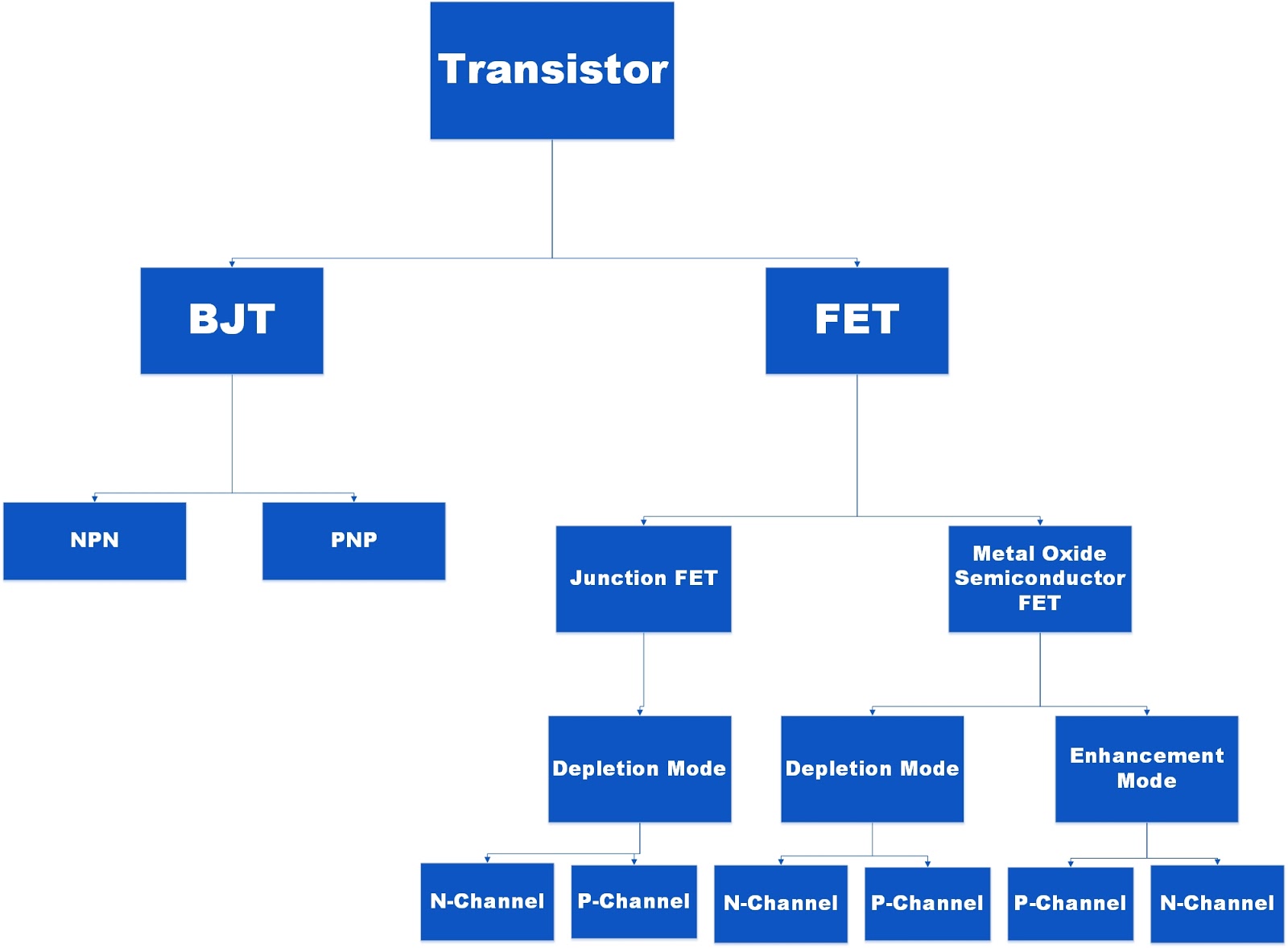
There two main types of Transistor,
  1. BJT Transistor (Bi Polar Junction)
  2. FETs Transistor(Field Effect Transistor)

BJT transistor are further classified to:
  1. n-p-n
  2. p-n-p

While FETs have also further classification.
The transistor tree below show classification of these Transistors.


Monday, 19 February 2018

Diode or pn junction:Definition, explanation, construction

Definition:


"Diode is an electrical component which allow the current to flow in one direction."

Explanation:


Diode is use to flow the current only in one direction and to block the current, if it flows in other direction. This property of blocking current in one direction and allowing it in only one direction is due to its construction which is explain below. It does not change the current, it just block the current to flow in other direction in a circuit. It is also use to convert AC source into DC source.
By blocking the negative interval and allowing only positive interval and by using some filter, decreases the fluctuation.

Construction:-


The diode is made up by the junction of two semiconductor of same material, lets suppose Silicon (Germanium could also be used). One semiconductor is doped with p type material which is boron and other semiconductor with n type material which is phosphorus. This junction is known as P-N junction. 
                                 
In P there is holes which is majority charge and in N there is electrons which is majority charge.
When we make junction of these (p-type and n-type) then holes which are majority charges in P, moves towards the N, and combine with the electrons, and majority charges in 
N which are electrons moves towards the P junction and combine with the holes.
 During this process there form a junction which is known as PN junction. Which consists both holes and electrons. And no more transfer of electrons and holes occurs(because of this junction wall.).

Working:


In electric Circuit, we take symbol for diode is, 


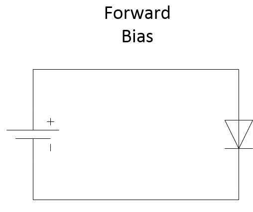
There are bias (applying any source) condition for semiconductor diode. Forward bias and Reverse bias. Diode works only in forward bias. In reverse bias, it blocks the flow of current in circuit or in other words. It becomes open circuit. which is its main property to allow current in only in one direction.


how to forward bias the diode?

We could do it by connecting positive terminal of voltage source from the anode and negative terminal with the cathode. And for reverse bias its vice versa.

How it allows current to flow in forward bias?


It allows current to flow in forward bias, because we connect positive terminal of voltage source with anode and it attracts electron from the N type. So electrons start to flow towards the anode terminal. And there is junction wall between diode, so to overcome there needs voltage of 0.3 or 0.7 . so could say that it is diode starting voltage.


How it blocks current in reverse bias? 


It blocks current in reverse bias, because the positive terminal of voltage source is connected with the cathode so it attracts electron towards cathode terminal so because of it, negative electrons from P type and positive holes from N type goes into junction and increases it. so junction widens and blocks the transfer.


Thursday, 4 January 2018

What is Charge, current, voltage? Definition explanation

Charge

Definition:

“Charge or Electrical charge is the property of, unit of a matter”

Explanation:

Charge does not physically exist; this is only a theoretical word. Yes, we use the word charge physically in many topics, just to describe the topic by taking a simple or basic thing (charge). Charge tells that how the matter will react with the other matter or in a magnetic field or in a electric field.
A matter is named as charge, only when there is a difference in number of electrons and number of protons in atom of that matter. If there are more electrons than proton in atom then it is negative charge and if there are more protons than electrons then it is positive charge. Hence this is two types of charge negative and positive charge.

Unit:-

The unit of charge is Coulomb and represented by q. 

Current

Definition:-

“Current is the rate of flow of electric charges.”

Explanation:-

Current is the flow of electric charges which is free electrons. Current flows in a circuit when there is pressure or some force applied to the charges in a circuit. Current flows from negative end to towards positive end. Rate of flow means, how much charges will flow in some fix time. There are two types of current. AC and DC.
AC means alternating current. The current which changes its direction of flow after half interval is known as alternating current.
DC means direct current. The current which flow in only one direction is known as DC current.
Each type of current has its own application.

Unit:-

Unit of current is A Ampere.
“When one coulomb charge will flow in one second through some point, then current will be one ampere.”

 Voltage

Definition:-

“Voltage is a force or pressure which causes the charges to flow through circuit.”

Explanation:

As we discuss in explanation section of current that , current flows through the circuit when some force or pressure applied to the charges in circuit. That force and pressure is Voltage. It is also known as potential difference. In some words, Voltage is the power of current. Means with how much power the current is flowing. The more the voltages the more the rate of flow of current in a circuit.

Unit:


Unit of voltage is V volt.

Wednesday, 3 January 2018

Electric Potential: definition, explanation, example.

Definition:

"Electric potential is the amount of word done in moving a point test charge from its original position(reference position) to some specific point or position, while moving the charge in direction opposite to direction of field in which charge is present."


Explanation:-

The definition above seem to be difficult to understand the electric potential but I will explain it briefly.
Consider their is a positive point charge A, which have its own electric field around it. And there is another positive test charge B which has no electric field.


 When we will move the test charge B towards the electric field of point charge A then test charge B will move away from the point charge A. This is natural that charge always move from high potential to low potential.


low potential is the area where the charge feels less force while high potential is the area where the force is high.


So to move charge, against its natural movements. we have to provide electric potential or force or to do work. To move test charge B towards the charge A we have to apply some potential which is electric potential, to move the charge from low potential to high potential. So charge B will gain potential energy while moving towards high potential from low potential.

Electric potential is the basic studies of charges behavior with each other. So if you feel there is some type of confusion feel free to comment. The post will be update!

Tuesday, 2 January 2018

Ampere's law: explanation, definition, formula

Definition:-

"Ampere's Law states that magnetic field around a conductor in which electric current is flowing, is directly proportional to the amount of electric current flowing through conductor."

Explanation:

Ampere's law provide us method or formula to calculate magnetic field, produced by electric current.
Just like electric field is directly proportional to the amount of charge, the magnetic field is directly proportional to the amount of electric current from which it is producing.

Formula:-

The most difficult in ampere's law is to derive its equation or make the formula for calculating the magnetic field around a long conducting wire.
So let's start this,
Consider we have long straight conducting wire, when electric current flows through it, the magnetic fields produces around the wire in concentric circle. As shown in below pic.


Every circle is for some specific part of wire and as we move forward in wire, the distance between these circles increases, that mean magnetic field is decreasing. Direction of magnetic field can be found by Fleming's right hand rule.(with direction of current giving)
Now to make the formula, consider there all the parts of wire( which have there magnetic field circuit) having length L and there magnetic field around these parts or elements is B for (every part).

So the equation will become,


And after removing proportionality,

where 𝝁 is the premiability of material or conductor.
B is the magnetic field and delta L is the sum of all length parts and I is the current flowing through the conductor,
sigma shows that the sum of all the length elements or parts with their magnetic field.
Where delta L could be replace by 2πr for particular(single part) length element.
So Then magnetic filed would become,

Saturday, 30 December 2017

Gauss's Law: definition, explanation, formula

Definition:

"Gauss's Law states that, Electric flux around a closed surface is depends upon charged enclosed in that surface and permittivity of free space."

Explanation:


Gauss's law states tell us about electric flux through some closed surface or area,
Electric flux through some area depends upon the charge enclosed by that area and the permittivity of free space in that area.
consider there is a closed sphere and there is charge enclosed in it, the flux out of it or the electric field out of the whole area could be determined with the help of Gauss's law.
Consider we wan to find the electric flux through the green planer area, then it will be simple that electric field lines multiplied by area perpendicular to the lines.
But when there comes a closed surface then there is nothing best except Gauss's law to find electric flux through closed surface (enclosed charge.)
It is not necessary that the surface should be closed sphere it could be any type of closed surface. And we will use Gauss's law to determine the electric flux through it.


Formula:


Mathematically we can determine the electric flux through closed surface by formula,

Where Q is the amount of charge enclosed and Ɛ is the permittivity of free space and 𝛟 is electric flux through the surface.


Electric Charge density, definition, explanation

Definition:

"Electric charge density is the amount of charge on unit volume space or surface or area."


Explanation:

Electric charge density is the density of charge on unit area, the charge could be less or  more, and charge could be positive or negative.
as shown in figure 1 below, in which there is positive charge on surface but less and on figure 2, there is more positive charge.
So area in figure 2 have more electric charge density than figure 1.
The area or volume could be one dimensional, two dimensional and three dimensional. 


Formula:

The electric charge density can be written in the form,
Where p is the charge density and q is the amount of charge and v is the volume of space and unit area. we can replace the v by A, when there is unit area.

Electric flux density, definition, explanation

Definition:

"Electric flux density is the electric flux passing through some unit area, and its direction is perpendicular to that unit area."

Explanation:

"Electric flux density", when we break down this sentence into "electric flux" and "density".
Then it is easy to understand that, the density of electric flux across some area. Consider there is a unit area shown below.


Electric flux is passing through this, in direction perpendicular to the unit area. The amount of electric flux passing through this unit area, in direction perpendicular to the unit area is called Electric flux density.


Formula:

When we write mathematically the electric flux density it is equal to the product of electric field E and permittivity of material.

                                                                           D=Ɛ.E
Unit:
The unit of electric flux density is coulombs per meter squared. 

Coulomb's law, definition explanation

Definition:-

"The magnitude of electrostatic force of attraction and the magnitude of electrostatic force of repulsion between two point charges is directly proportional to the product of magnitude of both charges and inversely proportional to the square of distance between them(both charges)."


Formula:-


mathematically we can write this in the form,
where F is the force,
q1 is the charge 1 and q2 is the charge 2,
and r is the distance between them.
this proportionality can be removed by placing proportionality constant k. in the formula, 

where the value of this constant depends upon the medium between the two point charges.
When there will be air then its value will be 9.0 x 10⁹ N • m2 / C2.
And this value of k will change, with the change in medium between the two charges.